 English
- English
-
 Español
 -
 Português
 -
 русский
 -
 Français
 -
 日本語
日本語 -
 Deutsch
 -
 tiếng Việt
 -
 Italiano
 -
 Nederlands
 -
 ภาษาไทย
 -
 Polski
 -
 한국어
한국어 -
 Svenska
 -
 magyar
 -
 Malay
Malay -
 বাংলা ভাষার
 -
 Dansk
Dansk -
 Suomi
Suomi -
 हिन्दी
 -
 Pilipino
 -
 Türkçe
 -
 Gaeilge
 -
 العربية
 -
 Indonesia
 -
 Norsk
Norsk -
 تمل
تمل -
 český
český -
 ελληνικά
 -
 український
 -
 Javanese
 -
 فارسی
فارسی -
 தமிழ்
தமிழ் -
 తెలుగు
 -
 नेपाली
 -
 Burmese
 -
 български
 -
 ລາວ
ລາວ -
 Latine
 -
 Қазақша
 -
 Euskal
 -
 Azərbaycan
 -
 Slovenský jazyk
 -
 Македонски
 -
 Lietuvos
 -
 Eesti Keel
 -
 Română
 -
 Slovenski


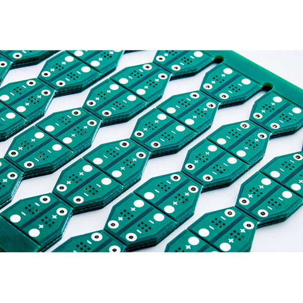
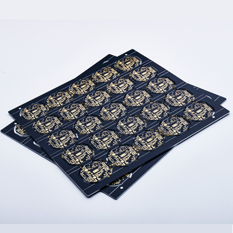
Multilayer PCB
Multilayer PCB board circuit boards are resistant to oxidation. Various structures, high density, and surface coating technologies ensure the quality and safety of circuit boards, which can be used with confidence. Multilayer PCB is mainly used in: consumer electronics, communication equipment, medical equipment, power supply and automotive electronics and other fields.
Send Inquiry
Product Description
Multilayer PCB
Multilayer PCB Product Introduction
Usually, the bare PCB board we see only sees the surface solder mask, PAD and silk screen characters, but we can't see the arrangement and number of layers of the lines inside. In fact, it is not as simple as you see. As PCB technology has improved and consumer demand for electronics has increased, multilayer PCB have gone from basic 2-layer boards to boards with 4, 6, and as many as 10 to 30 layers of dielectrics and conductors. Why increase the number of layers? Having more layers improves the board's ability to distribute power, reduce crosstalk, eliminate EMI, and support high-speed signals. The number of layers used for a multilayer PCB depends on the application, operating frequency, pin density, and signal layer requirements.
Usually, the bare PCB board we see only sees the surface solder mask, PAD and silk screen characters, but we can't see the arrangement and number of layers of the lines inside. In fact, it is not as simple as you see. As PCB technology has improved and consumer demand for electronics has increased, multilayer PCB have gone from basic 2-layer boards to boards with 4, 6, and as many as 10 to 30 layers of dielectrics and conductors. Why increase the number of layers? Having more layers improves the board's ability to distribute power, reduce crosstalk, eliminate EMI, and support high-speed signals. The number of layers used for a multilayer PCB depends on the application, operating frequency, pin density, and signal layer requirements.
Multilayer PCB Product Structure Diagram:

With a two-layer stack, the top layer (i.e. layer 1) is used as the signal layer. A 4-layer stack uses the top and bottom layers (or layers 1 and 4) as signal layers, and in this configuration, layers 2 and 3 are used as planes. The prepreg layer bonds two or more double-sided panels together and acts as a dielectric between the layers. A 6-layer PCB adds 2 copper layers, with layers 2 and 5 as planes. Layers 1, 3, 4 and 6 carry signals.
Moving on to the 6-layer structure, the inner layers 2 ~ 3 (when double-sided) and 4 ~ 5 (when double-sided) are core layers with prepreg (PP) sandwiched between the cores. Since the prepreg material is not fully cured, the material is softer than the core material. The multilayer PCB manufacturing process applies heat and pressure to the entire stack and melts the prepreg and fiber core so that the layers can bond together.
Multilayer PCB add more copper and dielectric layers to the stack. In an 8-layer PCB, the 7 inner rows of dielectric glue together the 4 plane layers and the 4 signal layers. 10- to 12-layer boards increase the number of dielectric layers, keep 4 plane layers, and increase the number of signal layers.
Schematic Diagram of the Front and Back of the Multi-layer PCB Product:

Multilayer PCB Product Manufacturing and Production Process Manufacturing Instructions:
| board | FR-4, High TG FR-4, Halogen Free FR-4, CEM1, CEM3, Aluminum PCB |
| layers | 1-40L |
| plate thickness | 0.3-4.0 mm |
| biggest size | 900X1220mm |
| Maximum Finished Copper Thickness | 12Oz |
| Etching tolerance | ±10% |
| Minimum line width | 0.075mm(3mil) |
| Minimum line spacing | 0.075mm(3mil) |
| Minimum aperture | 0.20mm |
| Board warpage | ≤ 0.75% |
| Impedance tolerance | ±10% |
| Minimum hole tolerance | ±0.05mm |
| Minimum Bore Tolerance (PTH) | ±0.075mm |
| Minimum Bore Tolerance (NPTH) | ±0.05mm |
| Minimum Panel Tolerance | ±0.10mm |
| Minimum punching tolerance | ±0.075mm |
| Minimum V-CUT Alignment Tolerance | ±0.10mm(4mil) |
| interlayer alignment | ±0.05mm(2mil) |
| Graphic registration tolerance | ±0.075mm(3mil) |
| Inspection test | AOI; electronic testing; high-speed flying probe |
| surface treatment | OSP;HASL;DNIG;FREE LEAD |
Multi-layer PCB products:
Consumer electronics, communication equipment , medical equipment , power supply and automotive electronics and other fields .
Advantages of multi-layer PCB products:
Multilayer PCB board circuit boards are resistant to oxidation. Various structures, high density, and surface coating technologies ensure the quality and safety of circuit boards, which can be used with confidence .
FAQ
Q1: I have a multi-layer PCB Gerber document and want to move some circuits and replace components, can you help me with it?
A1: Of course, we have senior PCB engineers. Multi-layer PCB design is our advantage. Please send Gerber information to pcb@jbmcpcb.com.
Q2: Most of the multi-layer PCB are even-numbered layers, and there are few odd-numbered layers?
A2: Yes, most of the PCB layers are even-numbered layers, such as the common 4L and 6L. Even-numbered layers are more advantageous than odd-numbered layers in terms of cost, structure and product stability.
Q3: We have too many electronic products in our lives. How to design a multi-layer PCB to reduce radiation?
A3: JBPCB has a senior team of more than 12 years, and has accumulated rich experience in PCB manufacturing from design, research and development to production. One of the measures to control the radiation source is to change the 2L PCB to 4L PCB. This is the basic characteristic of current. Be willing to choose the path with the lowest impedance.
Hot Tags: Multilayer PCB, China, Factory, Manufacturers, Suppliers, Price, Made in China
Related Categories
Send Inquiry
Please feel free to fill your inquiry in the form below. We will reply you in 24 hours.
Related Products


X
We use cookies to offer you a better browsing experience, analyze site traffic and personalize content. By using this site, you agree to our use of cookies.
Privacy Policy