 English
- English
-
 Español
 -
 Português
 -
 русский
 -
 Français
 -
 日本語
日本語 -
 Deutsch
 -
 tiếng Việt
 -
 Italiano
 -
 Nederlands
 -
 ภาษาไทย
 -
 Polski
 -
 한국어
한국어 -
 Svenska
 -
 magyar
 -
 Malay
Malay -
 বাংলা ভাষার
 -
 Dansk
Dansk -
 Suomi
Suomi -
 हिन्दी
 -
 Pilipino
 -
 Türkçe
 -
 Gaeilge
 -
 العربية
 -
 Indonesia
 -
 Norsk
Norsk -
 تمل
تمل -
 český
český -
 ελληνικά
 -
 український
 -
 Javanese
 -
 فارسی
فارسی -
 தமிழ்
தமிழ் -
 తెలుగు
 -
 नेपाली
 -
 Burmese
 -
 български
 -
 ລາວ
ລາວ -
 Latine
 -
 Қазақша
 -
 Euskal
 -
 Azərbaycan
 -
 Slovenský jazyk
 -
 Македонски
 -
 Lietuvos
 -
 Eesti Keel
 -
 Română
 -
 Slovenski


Thermoelectric Separation Copper Substrate PCB
You can rest assured to buy Jiubao Thermoelectric Separation Copper Substrate Pcb from our factory. Flashlight, industrial miner's lamp, automotive LED lamp, UV lamp, stage projection lamp, 5G communication, wall washer, LED street lamp, mechanical equipment and various precision and high-demand cooling lighting equipment
Send Inquiry
Product Description
Thermoelectric Separation Copper Substrate PCB
Thermoelectric Separation Copper Substrate PCB
Thermoelectric separation copper substrate pcb product introduction:
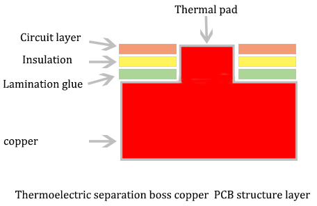
The thermal conductivity of copper in the metal core PCB manufacturing process is as high as 384W/(m·K), and the thermoelectric separation overcomes the shortcomings of insufficient heat conduction and heat dissipation of the existing single-sided copper substrate. The heat refers to the thermal pad (PAD), and the electricity refers to the positive and negative electrodes. The two are separated by insulating materials to form a special thermal pad. The function of the thermal pad is to conduct heat. The main function of the electrode is to conduct electricity. This packaging method is called thermoelectric separation. , its advantages are many, mainly in the LED heat dissipation design is very convenient. The large exposed copper area in the figure is designed as a large boss, which directly contacts the copper base and directly contacts the heat sink, and the heat is conducted out, which greatly improves the heat dissipation effect. The single-sided thermoelectric separation product can solve the problems of heat generation and light efficiency very well in the use of automobile lamps, and has the advantages of fast heat dissipation, high brightness, and energy saving.
The thermal conductivity of copper in the metal core PCB manufacturing process is as high as 384W/(m·K), and the thermoelectric separation overcomes the shortcomings of insufficient heat conduction and heat dissipation of the existing single-sided copper substrate. The heat refers to the thermal pad (PAD), and the electricity refers to the positive and negative electrodes. The two are separated by insulating materials to form a special thermal pad. The function of the thermal pad is to conduct heat. The main function of the electrode is to conduct electricity. This packaging method is called thermoelectric separation. , its advantages are many, mainly in the LED heat dissipation design is very convenient. The large exposed copper area in the figure is designed as a large boss, which directly contacts the copper base and directly contacts the heat sink, and the heat is conducted out, which greatly improves the heat dissipation effect. The single-sided thermoelectric separation product can solve the problems of heat generation and light efficiency very well in the use of automobile lamps, and has the advantages of fast heat dissipation, high brightness, and energy saving.
The formation process of thermoelectrically separated metal substrate pcb includes: sticking protective tape on one side of the copper base layer; forming anti-etching ink, exposure, development and etching through the circuit board process, so that the heat dissipation area forms a protrusion, and the height of the protrusion is equal to the insulating layer and the circuit layer. By stacking the circuit layer (copper foil) and the insulating layer (non-adhesive prepreg) together; opening a window in the heat dissipation area of the circuit layer and the insulating layer, which can be opened by die cutting or CNC forming; The heat dissipation layer, the circuit layer and the insulating layer (non-flow glue epoxy prepreg) are pressed together by hot pressing; the circuit layer circuit is produced according to the circuit board processing process, and the thermoelectric separation metal substrate provided by the utility model can be formed. . Thermoelectric separation is suitable for matching with a single high-power lamp bead, especially the COB package, so that the lamp can achieve better results.
Disadvantages of thermoelectrically separated copper substrate pcb: not suitable for single-electrode chip bare die packaging.
The thermoelectric separation copper substrate pcb structure is suitable for high-frequency circuits and areas with large changes in high and low temperatures, heat dissipation of precision communication equipment, and architectural decoration industries, as well as automotive LED lights, miner's lamps, and stage lights. Exposure equipment in industrial equipment and heat sinks of mining machines are all involved in applications.
Thermoelectric separation copper substrate pcb is divided into single-sided thermoelectric separation copper substrate pcb and double-sided thermoelectric separation copper substrate pcb, and now the single thermoelectric separation copper substrate pcb is introduced.
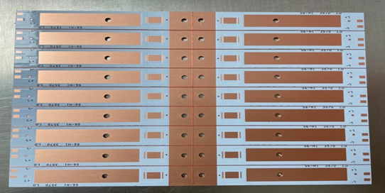
Thermoelectric Separation Copper Substrate PCB Product Structure Diagram:
Schematic Diagram of The Front and Back of The Thermoelectric Separation Copper Substrate Pcb Product:

Manufacturing Instructions for Copper Substrate Pcb Products and Production Processes:
| Base material | copper (C1100) |
| Layer count | 1L |
| Thickness(mm) | 0.4-5.0MM |
| Copper foil thickness(um) | 35/70/105/140um |
| Solder mask color | white/black/matte black/red/green/blue/matte green |
| Character Color | White/Black/Orange/Red/Blue |
| Forming method | CNC gong plate, CNC V cutting, mold forming, laser cutting and milling |
| Inspection test | AOI; high-speed flying probe; E-test; Voltage test |
| Surface treatment process | HASL FREE LEAD DNIG OSP |
| Delivery time | 5~6 days. |
Application Occasions of Copper Substrate Pcb Products:
Flashlight, industrial miner's lamp, automotive LED lamp, UV lamp, stage projection lamp, 5G communication, wall washer, LED street lamp, mechanical equipment and various precision and high-demand cooling lighting equipment
Advantages of Copper Substrate Pcb Products:
Long service life, efficient heat dissipation, stable application
FAQ
Q1. Are you a PCB manufacturer? Do you have a factory?
A: We are a professional printed circuit board manufacturer for more than 12 years, we have factories, machines, you can see our factory pictures.
Q2. Can I get PCB samples for free? Is free shipping available?
A: Yes, we can give you free PCB samples after talking and confirming all the details. But we don't offer free shipping, we will give you some discount if you buy a lot of products.
Q3. Do you do OEM?
Answer: Yes. We are a printed circuit board manufacturer, we have factories and dedicated automation equipment for the whole process of PCB and PCBA, and we can precisely detect and ship products. We provide one-stop purchasing service for PCB and PCBA.
Q4. Can a 2-layer thermal pad be in direct contact with the substrate, while the electrodes are on another layer of the PCB?
A: Yes, we can produce PCBs with 2-layer thermal conductive pads in direct contact with the substrate, we call it 2-layer thermoelectric separation copper substrate, you can see our product map, or you can send Gerber information to our email pcb@jbmcpcb. com to confirm.
Hot Tags: Thermoelectric Separation Copper Substrate PCB, China, Factory, Manufacturers, Suppliers, Price, Made in China
Send Inquiry
Please feel free to fill your inquiry in the form below. We will reply you in 24 hours.
Related Products


X
We use cookies to offer you a better browsing experience, analyze site traffic and personalize content. By using this site, you agree to our use of cookies.
Privacy Policy