 English
- English
-
 Español
 -
 Português
 -
 русский
 -
 Français
 -
 日本語
日本語 -
 Deutsch
 -
 tiếng Việt
 -
 Italiano
 -
 Nederlands
 -
 ภาษาไทย
 -
 Polski
 -
 한국어
한국어 -
 Svenska
 -
 magyar
 -
 Malay
Malay -
 বাংলা ভাষার
 -
 Dansk
Dansk -
 Suomi
Suomi -
 हिन्दी
 -
 Pilipino
 -
 Türkçe
 -
 Gaeilge
 -
 العربية
 -
 Indonesia
 -
 Norsk
Norsk -
 تمل
تمل -
 český
český -
 ελληνικά
 -
 український
 -
 Javanese
 -
 فارسی
فارسی -
 தமிழ்
தமிழ் -
 తెలుగు
 -
 नेपाली
 -
 Burmese
 -
 български
 -
 ລາວ
ລາວ -
 Latine
 -
 Қазақша
 -
 Euskal
 -
 Azərbaycan
 -
 Slovenský jazyk
 -
 Македонски
 -
 Lietuvos
 -
 Eesti Keel
 -
 Română
 -
 Slovenski


PCB multilayer circuit board manufacturing process
2025-08-04
The manufacturing process of circuit boards is a highly precise and complex process. The PCB multi-layer circuit board manufacturing process covers multiple steps from production to product, and each link has a decisive impact on the performance and quality of the final product.
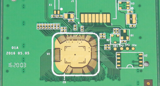
First, the manufacturing process is prepared according to the design documents, including the selection and pretreatment of the board material. Multilayer PCBs are typically constructed from layers of epoxy resin bonded to glass fibers. Each layer requires meticulous processing to ensure the flatness and cleanliness required for subsequent processing.
Next, the manufacturing process enters the pattern transfer stage, which involves transferring the design drawings to the PCB board. This step is typically accomplished through photolithography, where a lithography machine exposes the designed circuit pattern onto the PCB board, forming the desired conductive pattern.
Next, the etching process chemically removes the copper layer not covered by the photoresist, leaving only the conductive traces specified in the design. This step requires extremely high precision, as even the slightest error can affect circuit performance.
After the conductive traces are formed, the next step is drilling to prepare for interlayer connections on the multilayer PCB. The drilling process requires precise control of hole diameter and position to ensure accurate alignment between layers.
Next, the interlayer connection process begins, where a laminator connects the layers of board material with the conductive vias, forming a multilayer circuit structure. This step requires controlled temperature and pressure to ensure good electrical connections and mechanical strength after lamination.
Next comes surface treatment. Depending on the requirements of the final product, the PCB surface is treated with methods such as gold plating, tin plating, and OSP (organic over-protective film) to enhance wear resistance, corrosion resistance, and solderability.
Followed by a series of rigorous quality inspections, including dimensional inspection, conductivity testing, and thermal shock testing, each PCB meets quality standards. It is then packaged and prepared for delivery to customers.
The PCB multilayer circuit board manufacturing process is a complex one involving numerous precision processes. Each step requires precise control to ensure the high performance and reliability of the final product. From production to delivery, every step is a test of manufacturing process and a challenge to the technical skills of engineers. With the continuous advancement of electronic technology, the manufacturing process of multilayer PCB circuit boards is also constantly innovating and evolving to meet the growing demand for electronic devices. This process not only demonstrates the level of precision manufacturing in the electronics industry but also represents an essential micro-art in the modern electronic world.


X
We use cookies to offer you a better browsing experience, analyze site traffic and personalize content. By using this site, you agree to our use of cookies.
Privacy Policy