 English
- English
-
 Español
 -
 Português
 -
 русский
 -
 Français
 -
 日本語
日本語 -
 Deutsch
 -
 tiếng Việt
 -
 Italiano
 -
 Nederlands
 -
 ภาษาไทย
 -
 Polski
 -
 한국어
한국어 -
 Svenska
 -
 magyar
 -
 Malay
Malay -
 বাংলা ভাষার
 -
 Dansk
Dansk -
 Suomi
Suomi -
 हिन्दी
 -
 Pilipino
 -
 Türkçe
 -
 Gaeilge
 -
 العربية
 -
 Indonesia
 -
 Norsk
Norsk -
 تمل
تمل -
 český
český -
 ελληνικά
 -
 український
 -
 Javanese
 -
 فارسی
فارسی -
 தமிழ்
தமிழ் -
 తెలుగు
 -
 नेपाली
 -
 Burmese
 -
 български
 -
 ລາວ
ລາວ -
 Latine
 -
 Қазақша
 -
 Euskal
 -
 Azərbaycan
 -
 Slovenský jazyk
 -
 Македонски
 -
 Lietuvos
 -
 Eesti Keel
 -
 Română
 -
 Slovenski


PCB Design
As the professional manufacture, we would like to provide you Jiubao PCB Design. With the advent of the 5G era, PCB is an indispensable electronic product in our lives. People are becoming more refined and intelligent in electronic products, and their functions are becoming more and more powerful.
Send Inquiry
Product Description
Introduction to PCB Design:
As the professional manufacture, we would like to provide you Jiubao PCB Design. And we will offer you the best after-sale service and timely delivery. With the advent of the 5G era, PCB is an indispensable electronic product in our lives. People are becoming more refined and intelligent in electronic products, and their functions are becoming more and more powerful. Although the integration of chips is becoming more and more strict, the design requirements for circuit boards are also getting higher and higher, and PCB design is particularly important, which is related to the assembly and service life of electronic products.
Circuit board design, also called PCB design, because the full name of the circuit board (also called printed circuit board) in English is Printed circuit board, abbreviated as PCB, so the circuit board design is also called PCB design; circuit board design, from hand-drawing to more Large-scale component library, powerful automatic layout and routing and other functions make it more and more convenient for our engineers to design circuit boards.
Circuit board design, also called PCB design, because the full name of the circuit board (also called printed circuit board) in English is Printed circuit board, abbreviated as PCB, so the circuit board design is also called PCB design; circuit board design, from hand-drawing to more Large-scale component library, powerful automatic layout and routing and other functions make it more and more convenient for our engineers to design circuit boards.

The JBpcb R&D and design team comes from the fields of communication, smart equipment, and smart home design, and has rich design experience. Professionally committed to providing customers with related services of electronic product customization, providing complete one-stop service of PCB R&D design and PCBA processing.
PCB design software:
a) protel, Protel DXP, protel99se, Altium Designer
b)EAGLE layout
c) BORDSTATIONGoing and EE
d) Cadence spb software
e)PowerPCB, CAD, CAM350
The PCB is based on the circuit schematic diagram to realize the functions required by the circuit designer. The design of the PCB mainly refers to the circuit diagram design, which needs to consider various factors such as the layout of external connections, the optimal layout of internal electronic components, the optimal layout of metal connections and via, electromagnetic protection, and heat dissipation. Excellent circuit diagram design can save production costs and achieve good circuit performance and heat dissipation performance. Simple circuit diagram design can be realized by hand, and complex circuit diagram design needs to be realized with the help of computer-aided design.
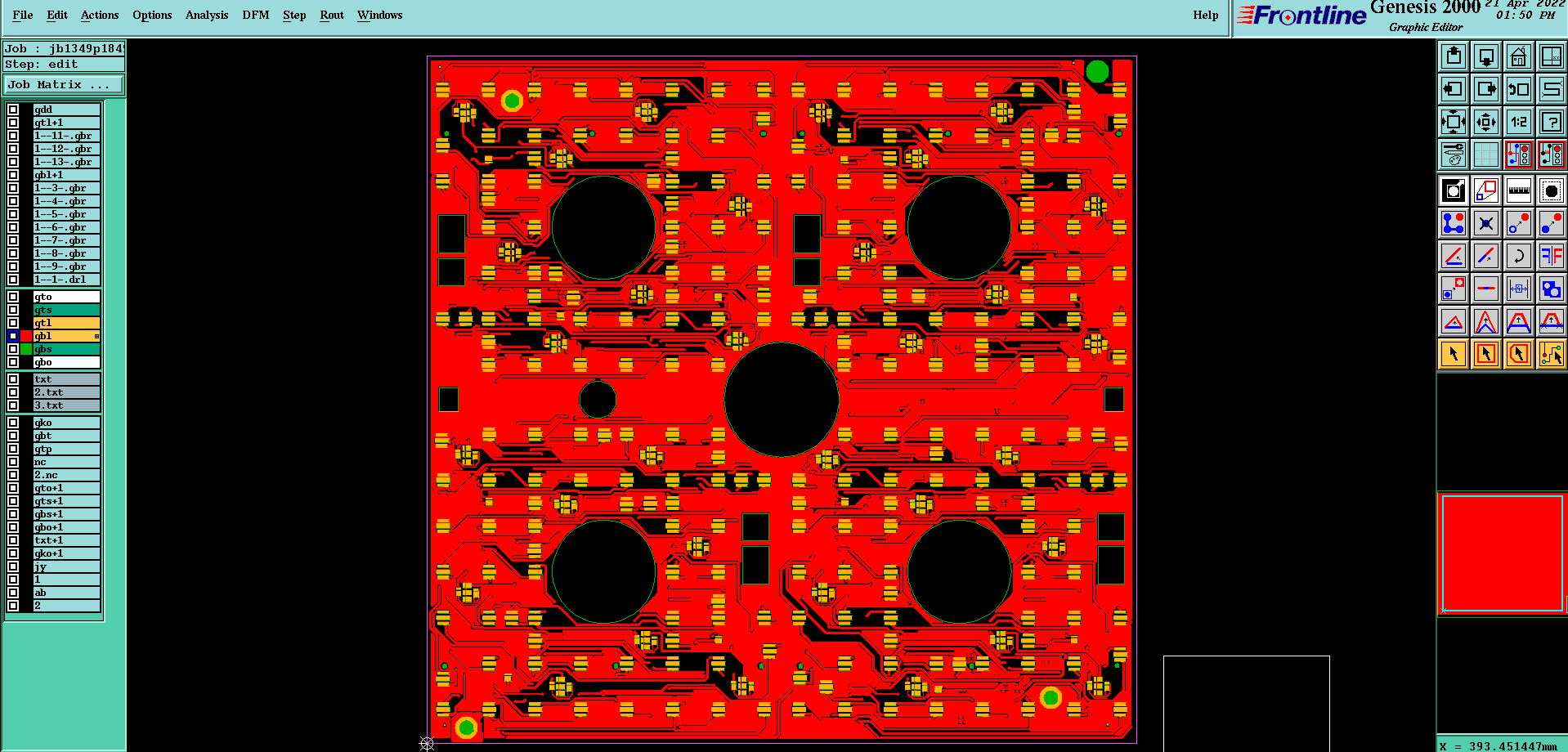
PCB design technology, including computer-aided manufacturing processing technology, namely CAD/CAM350, and light-painting technology. The following introduces the simple computer-aided manufacturing processing technology.
Computer-aided manufacturing (CAM350) is to carry out various processing according to the specified process. For the various process requirements mentioned above, necessary preparations must be made before light painting. For example, mirroring, solder mask expansion, process line, process frame, line width adjustment, center hole, outline, and other issues must be completed in the CAM350 process. Special attention should be paid to the places where the spacing is too small in the user file, and corresponding treatment must be made. Because the process flow and technical level of each factory are different, to meet the final requirements of users, necessary adjustments must be made in the production process to meet the requirements of users in terms of precision and other aspects. Therefore, CAM350 processing is an essential process in modern printed circuit manufacturing.
Computer-aided manufacturing (CAM350) is to carry out various processing according to the specified process. For the various process requirements mentioned above, necessary preparations must be made before light painting. For example, mirroring, solder mask expansion, process line, process frame, line width adjustment, center hole, outline, and other issues must be completed in the CAM350 process. Special attention should be paid to the places where the spacing is too small in the user file, and corresponding treatment must be made. Because the process flow and technical level of each factory are different, to meet the final requirements of users, necessary adjustments must be made in the production process to meet the requirements of users in terms of precision and other aspects. Therefore, CAM350 processing is an essential process in modern printed circuit manufacturing.
The Work Done by CAM350 for PCB Design
a) Correction of the size of the pad, combining the D code.
b) Correction of line width, combining D code.
c) Inspection of minimum spacing, between pads and pads, between pads and lines, and between lines and lines.
d) Inspection of the aperture size and combination.
e) Check of minimum line width.
f) Determine the solder mask expansion parameters.
g) Mirroring.
h) Add various craft lines and craft boxes.
i) Line width correction to correct for undercuts.
j) Forming a central hole.
k) Add outline corners.
l) Add positioning holes.
n) Imposition, rotation, mirroring.
m) Pieces.
o) Graphic superimposition processing, corner-cutting, and tangent processing. p) Add user logo.
FAQ
Q1: Are you a PCB source manufacturer?
A1: Yes, we are the source factory - OEM/ODM one-stop from PCB design to PCBA manufacturer.
Q2: What information do I need to provide for PCB design?
A2: a) Schematic: a complete electronic document format that can produce the correct netlist;
b) Mechanical dimensions: provide the specific position and direction identification of the positioning components, as well as the identification of the specific height limit position area;
c) Device packaging: provide component packaging library or electronic material specification;
d) Wiring Guidelines: Description of specific requirements for special signals, as well as design requirements such as impedance and stack-up.
Hot Tags: PCB Design, China, Factory, Manufacturers, Suppliers, Price, Made in China
Send Inquiry
Please feel free to fill your inquiry in the form below. We will reply you in 24 hours.
Related Products


X
We use cookies to offer you a better browsing experience, analyze site traffic and personalize content. By using this site, you agree to our use of cookies.
Privacy Policy