 English
- English
-
 Español
 -
 Português
 -
 русский
 -
 Français
 -
 日本語
日本語 -
 Deutsch
 -
 tiếng Việt
 -
 Italiano
 -
 Nederlands
 -
 ภาษาไทย
 -
 Polski
 -
 한국어
한국어 -
 Svenska
 -
 magyar
 -
 Malay
Malay -
 বাংলা ভাষার
 -
 Dansk
Dansk -
 Suomi
Suomi -
 हिन्दी
 -
 Pilipino
 -
 Türkçe
 -
 Gaeilge
 -
 العربية
 -
 Indonesia
 -
 Norsk
Norsk -
 تمل
تمل -
 český
český -
 ελληνικά
 -
 український
 -
 Javanese
 -
 فارسی
فارسی -
 தமிழ்
தமிழ் -
 తెలుగు
 -
 नेपाली
 -
 Burmese
 -
 български
 -
 ລາວ
ລາວ -
 Latine
 -
 Қазақша
 -
 Euskal
 -
 Azərbaycan
 -
 Slovenský jazyk
 -
 Македонски
 -
 Lietuvos
 -
 Eesti Keel
 -
 Română
 -
 Slovenski


Detailed PCB manufacturing process and related information
2023-08-26
PCB manufacturing process: first of all will be vice copper board cut into small pieces, and then coated with a layer of light-sensitive wet film, and sent to a machine through the template projecting ultraviolet light so that the line graphics appear in the inner layer of the new board, followed by sodium carbonate rinse will be line graphics other than all the graphic surfaces are removed and then optical inspection, and then PP semi-solid pictures and multiple memory of the new version of the dubbing stacked plate, and then under vacuum conditions to temperature Then we press the multilayer boards under vacuum condition by heating and pressing.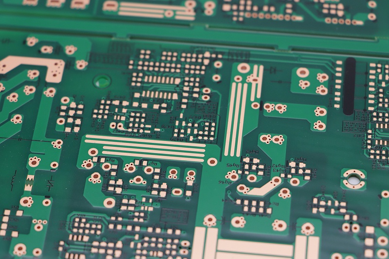
To make the electronic signals to each layer of the circuit board needs to be drilled in the circuit board as many as 2,000 small holes, these small holes are like the electronic signals to guide to the correct line entrance. After drilling the holes are successively copper immersion plate electricity and other processes to increase the electrical conductivity between the same layer, the next step is the outer layer of the graphic is generally after the photoluminescence of the graphic plating the outer layer of lithography and other processes and the inner layer of the graphic is basically the same, and then add solder resist for heating and baking the formation of a hard green layer of protection of the copper wires, the color of the resist layer can be selected at this stage, but manufacturers usually use the green color because it helps to check for defects, because it has high contrast and high quality, but also because it can be used to protect the copper wires. It has high contrast and trace visibility which is essential at the PCB prototyping stage.The color of the soldermask usually does not affect the functionality of the board, although darker colors are more heat-absorbent and therefore impractical for high-temperature applications. After the circuit board is soldered, the electronic assemblies are soldered in place, acting as alternating-current paths and junctions to direct the current to the correct circuit. Finally, the board is cut to shape and tested for performance according to the customer's needs, and then the board is complete.
PCB manufacturing is a detail-intensive process, and even simple mistakes can cost a company money due to faulty construction. When choosing your PCB manufacturing company, consider using a PCB manufacturer with a proven track record of success.
Our qualifications include: 1 hour response . One-on-one personalized service, ERP system . Full docking fast delivery, customized strength . Full automation control, imported raw materials. Strict quality control.
Previous:Benefits of Customized PCB Boards


X
We use cookies to offer you a better browsing experience, analyze site traffic and personalize content. By using this site, you agree to our use of cookies.
Privacy Policy