 English
- English
-
 Español
 -
 Português
 -
 русский
 -
 Français
 -
 日本語
日本語 -
 Deutsch
 -
 tiếng Việt
 -
 Italiano
 -
 Nederlands
 -
 ภาษาไทย
 -
 Polski
 -
 한국어
한국어 -
 Svenska
 -
 magyar
 -
 Malay
Malay -
 বাংলা ভাষার
 -
 Dansk
Dansk -
 Suomi
Suomi -
 हिन्दी
 -
 Pilipino
 -
 Türkçe
 -
 Gaeilge
 -
 العربية
 -
 Indonesia
 -
 Norsk
Norsk -
 تمل
تمل -
 český
český -
 ελληνικά
 -
 український
 -
 Javanese
 -
 فارسی
فارسی -
 தமிழ்
தமிழ் -
 తెలుగు
 -
 नेपाली
 -
 Burmese
 -
 български
 -
 ລາວ
ລາວ -
 Latine
 -
 Қазақша
 -
 Euskal
 -
 Azərbaycan
 -
 Slovenský jazyk
 -
 Македонски
 -
 Lietuvos
 -
 Eesti Keel
 -
 Română
 -
 Slovenski


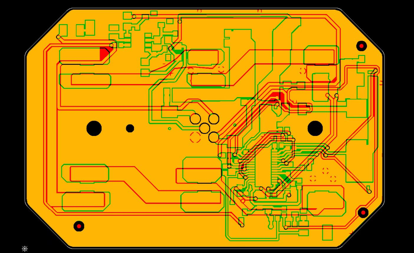
PCB Layout
In the entire PCB layout, the design process of the layout is the most limited, the skills are the smallest, and the workload is the largest. The quality of the PCB layout results will directly affect the effectiveness of the wiring, so it can be considered that a reasonable PCB layout is the first step to a successful PCB design.
Send Inquiry
Product Description
PCB Layout
Introduction to PCB Layout:
In the design, PCB layout is an important link. It can be said that the previous preparation work is done for it . In the entire PCB layout , the design process of the layout is the most limited, the skills are the smallest, and the workload is the largest. The quality of the PCB layout results will directly affect the effect of the wiring, so it can be considered that a reasonable PCB layout is the first step to a successful PCB design.
In particular, pre layout is a process of thinking about the structure of the entire circuit board, signal flow, heat dissipation, and structure. If the pre layout fails, all subsequent efforts will be in vain. PCB layout includes single-sided layout, double-sided layout and multi-layer layout. There are also two layout methods: automatic layout and interactive layout. Before automatic layout, you can use interactive layout to pre layout the lines with stricter requirements. The edges of the input end and the output end should be avoided to be adjacent and parallel to avoid reflection interference. If necessary, ground wire isolation should be added. The layout of two adjacent layers should be perpendicular to each other, and parasitic coupling will easily occur in parallel.
In particular, pre layout is a process of thinking about the structure of the entire circuit board, signal flow, heat dissipation, and structure. If the pre layout fails, all subsequent efforts will be in vain. PCB layout includes single-sided layout, double-sided layout and multi-layer layout. There are also two layout methods: automatic layout and interactive layout. Before automatic layout, you can use interactive layout to pre layout the lines with stricter requirements. The edges of the input end and the output end should be avoided to be adjacent and parallel to avoid reflection interference. If necessary, ground wire isolation should be added. The layout of two adjacent layers should be perpendicular to each other, and parasitic coupling will easily occur in parallel.
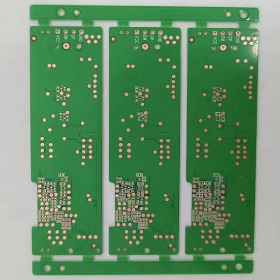
Schematic Diagram of Copper Substrate Pcb Product Structure:
The routing rate of automatic routing depends on good layout, and routing rules can be preset, including the number of bends of the routing, the number of via, the number of steps, and the like. Generally, the exploratory warp wiring is performed first, and the short lines are quickly connected, and then the labyrinth wiring is performed. And try re-wiring to improve the overall effect.
The current high-density PCB design has already felt that the through hole is not suitable, it wastes a lot of valuable wiring channels, in order to solve this contradiction, the blind hole and buried hole technology appeared, which not only completes the function of the through hole. , and also saves many wiring channels to make the wiring process more convenient, smoother and more complete. The design process of the PCB board is a complex and simple process. Only when people experience it for themselves can they get the true meaning of it.
The current high-density PCB design has already felt that the through hole is not suitable, it wastes a lot of valuable wiring channels, in order to solve this contradiction, the blind hole and buried hole technology appeared, which not only completes the function of the through hole. , and also saves many wiring channels to make the wiring process more convenient, smoother and more complete. The design process of the PCB board is a complex and simple process. Only when people experience it for themselves can they get the true meaning of it.
The PCB Layout Considers
the success of a product as a whole. One is to pay attention to the internal quality, and the other is to take into account the overall aesthetics. Only when both are perfect can the product be considered a success.
On a PCB board, the layout of components should be balanced, dense and orderly, and should not be top-heavy or heavy.
Will the PCB be deformed?
Do you reserve a craft edge?
Are MARK points reserved?
Do you need a puzzle?
How many layers can be guaranteed for impedance control, signal shielding, signal integrity, economy, achievability?
PCB Layout Eliminates low-level Errors
Does the printed board size match the processing drawing size? Can it meet the PCB manufacturing process requirements? Are there any positioning marks?
Are there any conflicts between components in two-dimensional and three-dimensional spaces?
Is the layout of components dense and orderly? Is it all finished?
Can components that need to be replaced frequently be easily replaced? Is the plug-in board easy to plug into the device?
Is there an appropriate distance between the thermal element and the heating element?
Is it easy to adjust the adjustable element?
Is there a radiator installed where heat dissipation is required? Is the air flow smooth?
Is the signal flow smooth and the interconnects shortest?
Do plugs, sockets, etc. contradict the mechanical design?
Has the interference problem of the line been considered?
PCB Layout Bypass Or Decoupling Capacitors
during PCB layout , and both require a bypass capacitor close to their power pins, typically 0.1µF. The pin should be as short as possible to reduce the inductive reactance of the trace, and it should be as close as possible to the device
The addition of bypass or decoupling capacitors on a circuit board, and the placement of these capacitors on the board, is common sense for both digital and analog designs, but their functions are different. In analog layout design, bypass capacitors are usually used to bypass high-frequency signals on the power supply. If bypass capacitors are not added, these high-frequency signals may enter sensitive analog chips through power pins. Generally, the frequencies of these high-frequency signals exceed the ability of the analog device to reject high-frequency signals. If bypass capacitors are not used in analog circuits, it can introduce noise and, in more severe cases, vibrations in the signal path. For digital devices such as controllers and processors, decoupling capacitors are also needed, but for different reasons. One function of these capacitors is to act as a "mini" charge bank, because in digital circuits, switching of gate states (i.e. switching on/off) typically requires large currents, and when switching, switching transient currents are generated on the chip and It is advantageous to have this extra "spare" charge flowing through the board. If there is not enough charge to perform the switching action, it will cause a large change in the supply voltage. Voltage variations that are too large can cause digital signal levels to go into indeterminate states and likely cause state machines in digital devices to behave incorrectly. The switching current flowing through the circuit board traces will cause the voltage to change. Due to the parasitic inductance of the circuit board traces, the following formula can be used to calculate the voltage change: V=Ldl/dt where V=voltage change L=circuit board travel Line inductance dI = change in current flowing through the trace dt = time to change in current Therefore, it is good to have a bypass (or decoupling) capacitor at the power supply or at the power supply pins of an active device for a number of reasons way of doing.
during PCB layout . If the current is relatively large, it is recommended to reduce the trace length and area, and do not run all over the field.
Switching noise on the input couples into the plane of the power supply output. The switching noise of the MOS tube of the output power supply affects the input power supply of the previous stage.
If there are a large number of high-current DCDC on the circuit board, there will be different frequencies, high-current and high-voltage jump interference.
Therefore, we need to reduce the area of the input power supply to meet the current flow. Therefore, when laying out the power supply, it is necessary to consider avoiding the full board running of the input power supply.

FAQ
Q1: How to check if the PCB layout is correct?
A1: a) Whether the size of the circuit board and the processing size required by the drawing are in line with each other.
b ) Whether the layout of the components is balanced and neatly arranged, and whether all the layouts have been completed.
c ) , whether there are conflicts at all levels. Such as components, frames, and whether the level that needs to be privately printed is reasonable.
d ) Whether the commonly used components are easy to use. Such as switches, plug-in board insertion equipment, components that need to be replaced frequently, etc.
e ) Whether the distance between thermal components and heating components is reasonable.
f ) , whether the heat dissipation is good.
g ) , whether the interference of the line needs to be considered
Q2: What are the PCB layout setting skills ?
The design requires different grid settings at different stages. In the layout stage, large grid points can be used for device layout; for large devices such as ICs and non-positioning connectors, a grid point accuracy of 50~100 mil can be used for layout, while for resistors Small passive components such as capacitors and inductors can be laid out using a 25mil grid. The accuracy of the large grid points facilitates device alignment and layout aesthetics.
Q3: What are PCB layout rules ?
A3:a ) Under normal circumstances, all components should be arranged on the same side of the circuit board. Only when the top components are too dense, some devices with limited height and low heat generation, such as chip resistors and chip capacitors, can be placed , SMD IC, etc. are placed in the lower layer.
b ) Under the premise of ensuring the electrical performance, the components should be placed on the grid and arranged in parallel or perpendicular to each other, so as to be neat and beautiful. In general, the overlapping of components is not allowed; the arrangement of components should be compact, and the components should be on the entire layout. It should be evenly distributed and consistent in density.
c ) The minimum spacing between adjacent pad patterns of different components on the circuit board should be more than 1MM.
d ), the distance from the edge of the circuit board is generally not less than 2MM. The best shape of the circuit board is a rectangle, and the aspect ratio is 3:2 or 4:3. When the surface size of the circuit board is greater than 200MM by 150MM, it should be considered that the circuit board can withstand mechanical strength.
Q4: What is the PCB layout placement order ?
A4: a ) Place components that are closely matched with the structure, such as power sockets, indicator lights, switches, connectors, etc.
b ) Place special components, such as large components, heavy components, heating components, transformers, ICs, etc.
c ) Place small components.
Hot Tags: PCB Layout, China, Factory, Manufacturers, Suppliers, Price, Made in China
Send Inquiry
Please feel free to fill your inquiry in the form below. We will reply you in 24 hours.
Related Products


X
We use cookies to offer you a better browsing experience, analyze site traffic and personalize content. By using this site, you agree to our use of cookies.
Privacy Policy