 English
- English
-
 Español
 -
 Português
 -
 русский
 -
 Français
 -
 日本語
日本語 -
 Deutsch
 -
 tiếng Việt
 -
 Italiano
 -
 Nederlands
 -
 ภาษาไทย
 -
 Polski
 -
 한국어
한국어 -
 Svenska
 -
 magyar
 -
 Malay
Malay -
 বাংলা ভাষার
 -
 Dansk
Dansk -
 Suomi
Suomi -
 हिन्दी
 -
 Pilipino
 -
 Türkçe
 -
 Gaeilge
 -
 العربية
 -
 Indonesia
 -
 Norsk
Norsk -
 تمل
تمل -
 český
český -
 ελληνικά
 -
 український
 -
 Javanese
 -
 فارسی
فارسی -
 தமிழ்
தமிழ் -
 తెలుగు
 -
 नेपाली
 -
 Burmese
 -
 български
 -
 ລາວ
ລາວ -
 Latine
 -
 Қазақша
 -
 Euskal
 -
 Azərbaycan
 -
 Slovenský jazyk
 -
 Македонски
 -
 Lietuvos
 -
 Eesti Keel
 -
 Română
 -
 Slovenski


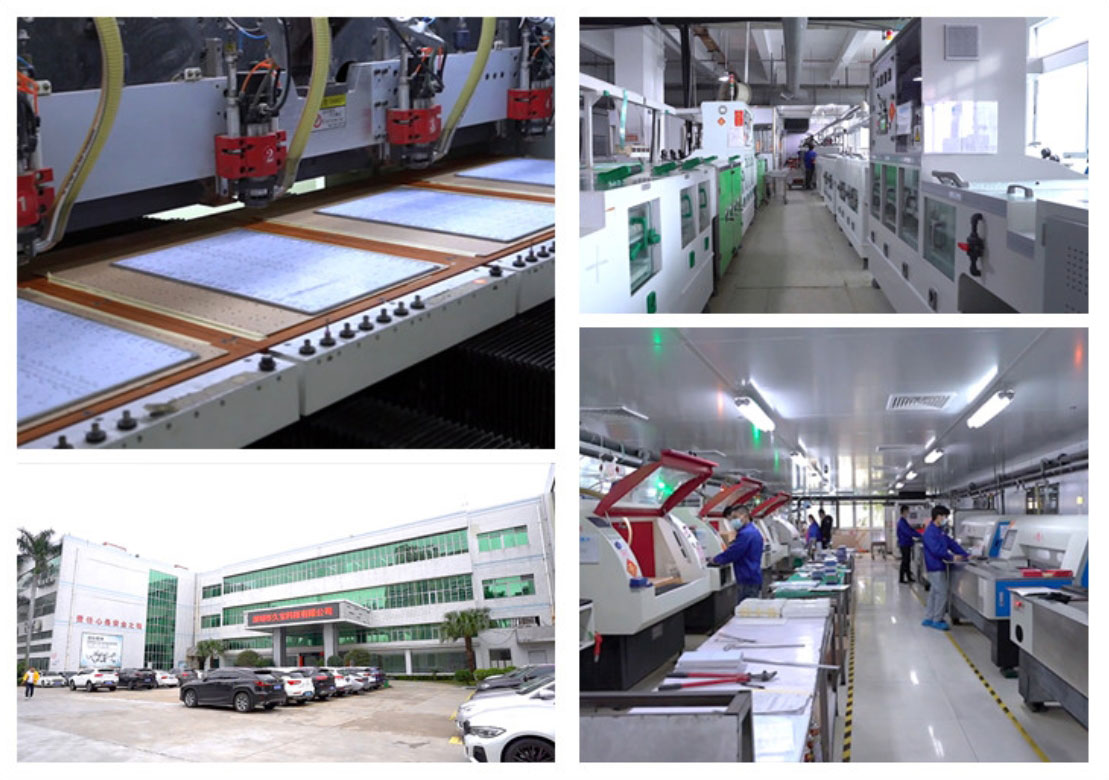
PCB circuit board manufacturers take a look at the production of circuit boards
2023-11-09
PCB circuit board manufacturers take a look at the production of circuit boards
PCB board line graphics, that is, PCB circuit board manufacturers using exposure imaging and development etching process technology to complete, whether it is a PCB multilayer circuit boards, or flexible circuit boards, in the production of line graphics have to use exposure imaging and development process technology. Below let JBpcb to introduce the two processes in detail the processing characteristics and processing principles
Exposure: Due to the coated PCB circuit board substrate on the insulating medium layer thickness is thicker, therefore, to use a larger rate of exposure machine on the PCB circuit board exposure, such as the use of 7 kilowatts of metal halide (such as tungsten lamps) lamps and in the line with parallel (or reflection of good quasi-parallel light) exposure machine. The amount of light on the surface of the dried insulating dielectric layer should be between 200 and 250, and its exposure time can be carried out and adjusted by the optical ladder scale table and other tests or conditions provided by the supplier, and generally should be used for a larger amount of exposure and shorter exposure time. For the use of low-power exposure machine, due to low light energy, resulting in a long exposure time, then the light refraction, diffraction and other aggravation, which is unfavorable for the manufacture of fine pitch or high-density interconnections of the guide hole.
Developing and cleaning: developing and cleaning conditions and liquid photoresist solder resist ink is similar to the situation and conditions. Attention should be paid to the concentration of sodium carbonate in the developing solution and temperature changes, often adjust the development time (or transfer speed) or adjust the solution, which is related to the PCB circuit board graphics development whether the problem of thorough and clean.
Curing (heat curing and UV curing). PCB circuit board after exposure development, although the photochemical (cross-chaining) effect through the exposure, basically cured, but most of them are not complete. Coupled with the development, cleaning and other absorbed water, so to be completed by heating. On the one hand, water and solvents can be removed, on the other hand, mainly to make the curing further completion and deepening.
But heat curing is mostly carried out by conduction heat. Therefore, the curing is carried out or completed gradually from the surface to the interior, so it is a gradient type of curing degree state. However, because UV light has the property of penetrating substances, and because epoxy resins and the like have the property of strongly absorbing UV light, they have a strong photocrosslinking reaction, which results in the complete curing and the thorough expulsion of organic solvent substances. Therefore, the insulating dielectric layer for laminated panels must be fully cured and the water and solvent must be thoroughly removed in order to achieve the expected Tg (fiberglassing temperature) and }dielectric constant requirements. Therefore, in the curing of most of the heat curing and then UV curing of these two steps, in order to thoroughly cured Note that the curing should be strictly controlled. Should be based on experiments and tests to set the control time, PCB circuit boards if over-curing or under-curing will cause deterioration of product performance and change the roughness (brushing) phenomenon. This will bring a lot of quality hazards to the back of the plating process.
By up to a long time of practical experience, nowadays PCB circuit board manufacturers in the exposure and development process will have strict control of technical parameters. jbpcb has been to produce high-quality, high-efficiency, high-volume PCB circuit board as the goal of the exposure and development process has been more than 13 years of accumulation of technology, such as you are interested in cooperation, welcome to contact us.


X
We use cookies to offer you a better browsing experience, analyze site traffic and personalize content. By using this site, you agree to our use of cookies.
Privacy Policy