 English
- English
-
 Español
 -
 Português
 -
 русский
 -
 Français
 -
 日本語
日本語 -
 Deutsch
 -
 tiếng Việt
 -
 Italiano
 -
 Nederlands
 -
 ภาษาไทย
 -
 Polski
 -
 한국어
한국어 -
 Svenska
 -
 magyar
 -
 Malay
Malay -
 বাংলা ভাষার
 -
 Dansk
Dansk -
 Suomi
Suomi -
 हिन्दी
 -
 Pilipino
 -
 Türkçe
 -
 Gaeilge
 -
 العربية
 -
 Indonesia
 -
 Norsk
Norsk -
 تمل
تمل -
 český
český -
 ελληνικά
 -
 український
 -
 Javanese
 -
 فارسی
فارسی -
 தமிழ்
தமிழ் -
 తెలుగు
 -
 नेपाली
 -
 Burmese
 -
 български
 -
 ລາວ
ລາວ -
 Latine
 -
 Қазақша
 -
 Euskal
 -
 Azərbaycan
 -
 Slovenský jazyk
 -
 Македонски
 -
 Lietuvos
 -
 Eesti Keel
 -
 Română
 -
 Slovenski


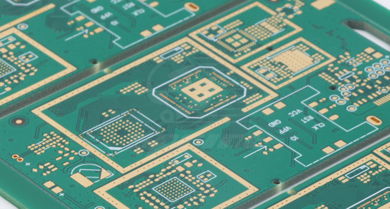
High-density multi-layer PCB board solution
2025-07-10
As electronic devices develop towards smaller size and higher performance, the density and complexity of circuit boards are becoming increasingly demanded. The "high-density multi-layer PCB solution" was born to meet this challenge, providing an effective way to solve precision electronic design problems for multiple industries. The following is a detailed introduction to the advantages of the high-density multi-layer PCB solution and what industry problems it solves.
Industry problems solved by high-density multi-layer PCB board solutions
1. Consumer electronics industry: Smartphones, tablets and other devices need to integrate more functions and higher performance in a limited space. High-density multi-layer PCB board solutions can achieve more compact circuit design.
2. Medical equipment industry: High-precision medical monitoring and diagnostic equipment rely on complex electronic components and precise signal processing. High-density multi-layer PCB boards can provide the necessary design flexibility and performance.
3. Aerospace industry: For electronic systems that need to work stably in extreme environments, high-density multi-layer PCB board solutions can provide higher reliability and durability.
4. Automotive electronics industry: Advanced driver assistance systems (ADAS) and infotainment systems used in modern cars require high-performance electronic control units. High-density multi-layer PCB boards are the key to realizing these systems.
5. Industrial automation: The development of automated control systems and robotics requires more efficient data processing and signal transmission capabilities. High-density multi-layer PCB board solutions can meet these needs.
Advantages of high-density multi-layer PCB solutions
1. Space optimization: By increasing the number of layers of the circuit board and optimizing the routing design, more circuit functions can be realized in a smaller space.
2. Performance improvement: Multi-layer PCBs can provide shorter signal transmission paths, reduce signal delays and interference, and improve the performance of electronic devices.
3. Design flexibility: High-density multi-layer PCBs allow designers to design creatively in three-dimensional space and achieve more complex circuit layouts.
4. Enhanced reliability: The structure of multi-layer PCBs is more stable, which can better resist physical shocks and environmental changes, and improve the durability of products.
5. Thermal management: Through reasonable inter-layer layout and thermal management design, high-density multi-layer PCBs can more effectively disperse heat and ensure stable operation of equipment.
6. Cost-effectiveness: Although the manufacturing cost of high-density multi-layer PCBs may be high, the performance improvement and market competitiveness it brings can save costs for enterprises in the long run.
High-density multi-layer PCB solutions are an effective means to meet the challenges of modern electronic design. It provides strong support for electronic equipment design in various industries by providing advantages such as space optimization, performance improvement, enhanced design flexibility, reliability guarantee and effective thermal management. With the continuous advancement of technology and the growing market demand, high-density multi-layer PCB board solutions will continue to promote innovation and development in the electronics industry and meet the future demand for high-performance electronic devices.


X
We use cookies to offer you a better browsing experience, analyze site traffic and personalize content. By using this site, you agree to our use of cookies.
Privacy Policy