 English
- English
-
 Español
 -
 Português
 -
 русский
 -
 Français
 -
 日本語
日本語 -
 Deutsch
 -
 tiếng Việt
 -
 Italiano
 -
 Nederlands
 -
 ภาษาไทย
 -
 Polski
 -
 한국어
한국어 -
 Svenska
 -
 magyar
 -
 Malay
Malay -
 বাংলা ভাষার
 -
 Dansk
Dansk -
 Suomi
Suomi -
 हिन्दी
 -
 Pilipino
 -
 Türkçe
 -
 Gaeilge
 -
 العربية
 -
 Indonesia
 -
 Norsk
Norsk -
 تمل
تمل -
 český
český -
 ελληνικά
 -
 український
 -
 Javanese
 -
 فارسی
فارسی -
 தமிழ்
தமிழ் -
 తెలుగు
 -
 नेपाली
 -
 Burmese
 -
 български
 -
 ລາວ
ລາວ -
 Latine
 -
 Қазақша
 -
 Euskal
 -
 Azərbaycan
 -
 Slovenský jazyk
 -
 Македонски
 -
 Lietuvos
 -
 Eesti Keel
 -
 Română
 -
 Slovenski


On the role of X-ray in PCB circuit board inspection
2023-10-20
In recent years, X-RAY ray three-dimensional fluoroscopic imaging inspection technology 3D X-RAY to the rapid development, and step by step to develop into a high degree of integration of electronic devices manufacturing industry must be detected. Many people may not understand the X-RAY in the circuit board inspection is to play what role, jiubao circuit editorial today to take you to understand:
X-ray three-dimensional perspective imaging detection technology compared to the traditional X-ray two-dimensional imaging detection X-RAY, it can be a full range of non-blind reproduction of the internal structure of the test object, there will be no structural image overlap phenomenon, in the form of two-dimensional tomographic images or three-dimensional stereo image of the defects to accurately locate and determine the information is perfect, in the field of micronanufacturing technology, electronic device science and other areas of very important and common use.
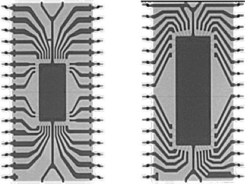
PCB manufacturers in the BGA components after the completion of welding, because of its solder joints by the components themselves covered, and therefore can not be used in the traditional visual inspection of the solder joints of the welding quality, but also can not be used to automate the optical inspection instruments on the surface of the solder joints to do quality judgment. In order to achieve a useful inspection, the solder joints of BGA components can be inspected in three dimensions with X-ray inspection equipment, where the specification, shape, hue and saturation of the BGA solder balls are uniform and the internal structural defects of the solder balls are clearly visible.
3D X-ray three-dimensional perspective imaging makes the electronic device manufacturing quality inspection method has triggered a new change, which is the current stage of the thirst to further enhance the level of manufacturing technology, improve manufacturing quality, and timely handling of electronic device assembly problems as a breakthrough in the solution of the producer's choice, and along with the development of electronic component packaging, other ways to detect equipment failures because of its limitations. With the development of electronic component packaging, other ways of detecting equipment failures because of its limitations and struggling, Honglian circuit I believe that the X-ray three-dimensional fluoroscopic imaging inspection equipment will become the new focus of electronic component packaging production equipment, and plays an important role in its manufacturing field.


We use cookies to offer you a better browsing experience, analyze site traffic and personalize content. By using this site, you agree to our use of cookies.
Privacy Policy