 English
- English
-
 Español
 -
 Português
 -
 русский
 -
 Français
 -
 日本語
日本語 -
 Deutsch
 -
 tiếng Việt
 -
 Italiano
 -
 Nederlands
 -
 ภาษาไทย
 -
 Polski
 -
 한국어
한국어 -
 Svenska
 -
 magyar
 -
 Malay
Malay -
 বাংলা ভাষার
 -
 Dansk
Dansk -
 Suomi
Suomi -
 हिन्दी
 -
 Pilipino
 -
 Türkçe
 -
 Gaeilge
 -
 العربية
 -
 Indonesia
 -
 Norsk
Norsk -
 تمل
تمل -
 český
český -
 ελληνικά
 -
 український
 -
 Javanese
 -
 فارسی
فارسی -
 தமிழ்
தமிழ் -
 తెలుగు
 -
 नेपाली
 -
 Burmese
 -
 български
 -
 ລາວ
ລາວ -
 Latine
 -
 Қазақша
 -
 Euskal
 -
 Azərbaycan
 -
 Slovenský jazyk
 -
 Македонски
 -
 Lietuvos
 -
 Eesti Keel
 -
 Română
 -
 Slovenski


What is PCB Design?
2023-06-15
Definition of PCB Design
What is PCB design? PCB design refers to the process of converting circuit schematics into actual circuit boards. It includes a series of tasks such as circuit layout, component selection, routing planning, and electrical characteristic analysis. The purpose of PCB design is to achieve circuit reliability, stability and performance optimization. It is an integral part of the manufacturing process of electronic products and one of the necessary skills for electronic engineers. The definition of PCB design is the process of converting circuit schematics into actual circuit boards. It involves all aspects of electronic engineering and requires engineers to have solid circuit knowledge, skilled design skills, and rich practical experience. The quality of PCB design directly affects the performance and reliability of electronic products, so it plays an important role in the manufacturing process of electronic products.
Process of PCB design
1. PCB is the abbreviation of Printed Circuit Board, that is, printed circuit board, which is the carrier of electronic components. PCB design is to convert the circuit diagram into the actual circuit board layout to realize the function of the circuit.
2. The process of PCB design generally includes the following steps:
(1) Schematic design: carry out circuit design according to the circuit schematic diagram.
(2) Package design: Select the appropriate component package and carry out package design.
(3) Layout design: According to the circuit schematic diagram and packaging design, carry out the layout design of the circuit board.
(4) Routing design: According to the layout design of the circuit board, carry out the wiring design of the circuit board.
(5) Output manufacturing files: convert PCB design files into manufacturing files for manufacturing.
(6) PCB manufacturing: PCB manufacturing is carried out according to the manufacturing documents.
(7) Welding and testing: Welding the components to the PCB, and testing and debugging. The above is the basic process of PCB design, different projects may be different. In actual operation, it needs to be adjusted and optimized according to the specific situation to achieve the best PCB design effect.
Considerations in PCB Design
Precautions in PCB design
1. Component selection: To select components with reliable quality and stable performance, at the same time, pay attention to whether the size and pin spacing of components meets the requirements of the circuit board layout.
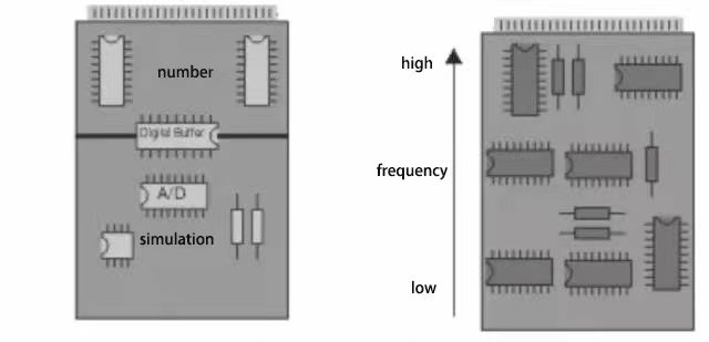
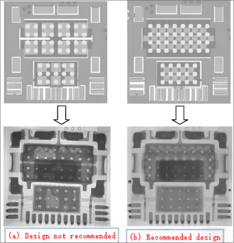
2. Circuit board layout: Reasonable layout of various components is required to make the circuit board compact, beautiful, and easy to manufacture and maintain. At the same time, factors such as line length and signal interference need to be considered.
3. Wiring: According to the requirements of circuit design, each signal line should be reasonably arranged to avoid signal interference and mutual interference. At the same time, pay attention to the setting of parameters such as line width and line spacing.
4. Production: Pay attention to ensuring the quality of the circuit board during the production process, such as preventing corrosion and maintaining circuit accuracy. At the same time, we must also pay attention to safe production, such as preventing chemical poisoning.
5. Inspection: After the production is completed, the circuit board shall be inspected to ensure that the performance of the circuit board meets the design requirements. In short, in PCB design, we must pay attention to reasonable material selection, reasonable layout, reasonable wiring, ensure production quality and conduct strict testing, in order to produce high-quality and reliable circuit boards.
Application field of PCB design
JBpcb has a team of senior engineers with 13 years of experience. Engineers need to consider circuit reliability, stability, wiring rationality, electromagnetic compatibility, and other factors when designing to ensure the normal operation of the circuit. Application fields of PCB design are widely used in the manufacturing process of electronic products, such as computers, mobile phones, TVs, etc. At the same time, PCB design is also used in industrial control, medical equipment, aerospace, and other fields to meet the requirements for circuit reliability, stability, and high density. With the continuous advancement of technology, PCB design is gradually developing in the direction of high speed, high frequency, high density, multi-layer, and flexibility, providing better solutions for electronic products in various industries.


We use cookies to offer you a better browsing experience, analyze site traffic and personalize content. By using this site, you agree to our use of cookies.
Privacy Policy